
The evolution of circuits is an interesting topic for all electronics enthusiasts. Although the basic idea invented in the 1800s still works today, there are certainly a lot of advancements over the years.
The bulkiness of some circuits has dramatically reduced, thanks to printed circuit boards (PCB). Modern PCBs can hold thousands of components in the smallest space possible. They’ve also enhanced the creation of futuristic devices, such as flexible electronics that are ideal for various tasks.
But what are these PCBs, and how do they work? The article will answer this question and discuss some of the main parts of these boards.
What Is A Printed Circuit Board?
A PCB is a thin board that contains conductive pathways etched onto its surface. The paths connect electronic components mounted on the PCB electrically.
Some call it a printed wiring card, but this was relevant to the method before the advent of modern technology. Circuit construction required the point-to-point wiring technique, which was laborious and prone to frequent failures.
On the other hand, modern PCBs are compact and efficient, allowing multiple components to be placed on a single board. This reduces the size and complexity of the overall device.
It’s worth noting that there are different types of PCBs, and their popularity depends on specific applications and performance requirements. Here are some of the most common designs:
- Double-Sided PCBs
They have circuit pathways on both sides. Manufacturers use these PCBs mostly in computers, automotive devices, and other consumer electronics.
- Multilayer PCBs
These printed circuits consist of at least three conductive materials. Their design is ideal for high-performance electronics such as medical equipment, communication devices, and aerospace systems.
- HDI PCBs
High-density interconnector boards have many wiring connections and finer spaces per unit area. Their ability to park more functionality in a smaller space makes them ideal for portable electronics like tablets and smartphones.
- Rigid PCBs
As the name suggests, these PCBs are designed with materials that give them a solid structure. Pretty much all consumer electronics use these products.
- Thin-Film PCBs
These PCBs are made from the same materials as rigid PCBs. However, the composition of these materials allows for flexibility. They’re common in applications where the PCB must be bent or shaped—for example, wearable devices and medical sensors.
Thin-film technology has rapidly grown over the past few years and is one of today’s most significant innovations. Several articles like https://korvustech.com/thin-film-circuit-board/ are posted online for you to learn more about this futuristic idea.
Basic Parts Of PCBs
Of course, most of the PCBs mentioned above have different material compositions, and the specifics depend on their applications. However, they all share the following essential parts:
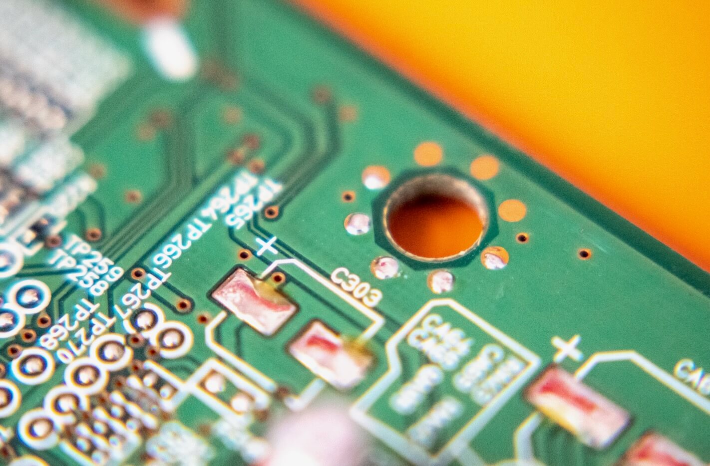
- Conductive pathways
Every PCB contains thin lines of copper called conductive pathways or traces. These pathways are created through etching, which removes the unwanted copper from the board to leave only the desired traces.
They connect the different components on the board to complete the circuits. The width and spacing of the traces depend on the current-carrying capacity and the required impedance.
- Substrate
The substrate is the base material that holds the traces and supports the mounted electronic components. It also offers insulation between different layers of the circuit.
Fiberglass-reinforced epoxy resin, or flame-retardant level 4 (FR-4), is the most common substrate material. It’s lightweight, durable, and has excellent electrical and thermal insulation properties.
Other popular alternatives include polyimide, flame retardant level 2 (FR-2), low-temperature co-fired ceramics (LTCC), Teflon, and flexible substrates.
- Pads
The circuit designers leave small areas of exposed copper on the PCB for connecting electronic components. These spots are called pads and are usually rectangular or circular for easy mounting. Their sizes also vary with the components being soldered.
- Solder
Solder is a metal alloy used to mount electronic components to the pads through a process called soldering. It’s usually a mixture of lead and tin, but there is also lead-free solder. This material is used to create a permanent, low-resistance electrical connection between the PCB and component terminals.
- Silkscreen
The silkscreen is a layer of ink printed onto the PCB. It is used to label the components, reference numbers, and other information. This layer typically includes text, symbols, and other markings that help identify the components and their locations on the board. The silkscreen layer also indicates polarities, which are vital for proper circuit operation.
Conclusion
Printed circuit technology has evolved significantly over the past few years. Some of the essential parts of modern PCBs include a substrate, which can either be FR-4, FR-2, Teflon, or TCC. Other features are conductive pathways, silkscreen, pads, and solder. Remember, the design and composition of these materials depend on the desired application and performance level.